Quantum leap!
This isn’t just another lab experiment. We’re talking about pulling quantum computing out of the theoretical ether and firmly planting it onto the same industrial highway that’s currently building the AI processors of tomorrow. Belgian research giant imec has just unveiled what they’re calling the world’s first quantum dot qubit device, and the kicker? It’s fabricated using High-NA EUV lithography – the absolute bleeding edge of semiconductor manufacturing. Think of it like a Formula 1 engine being built on the same assembly line as your next everyday sedan; it radically compresses timelines and expectations.
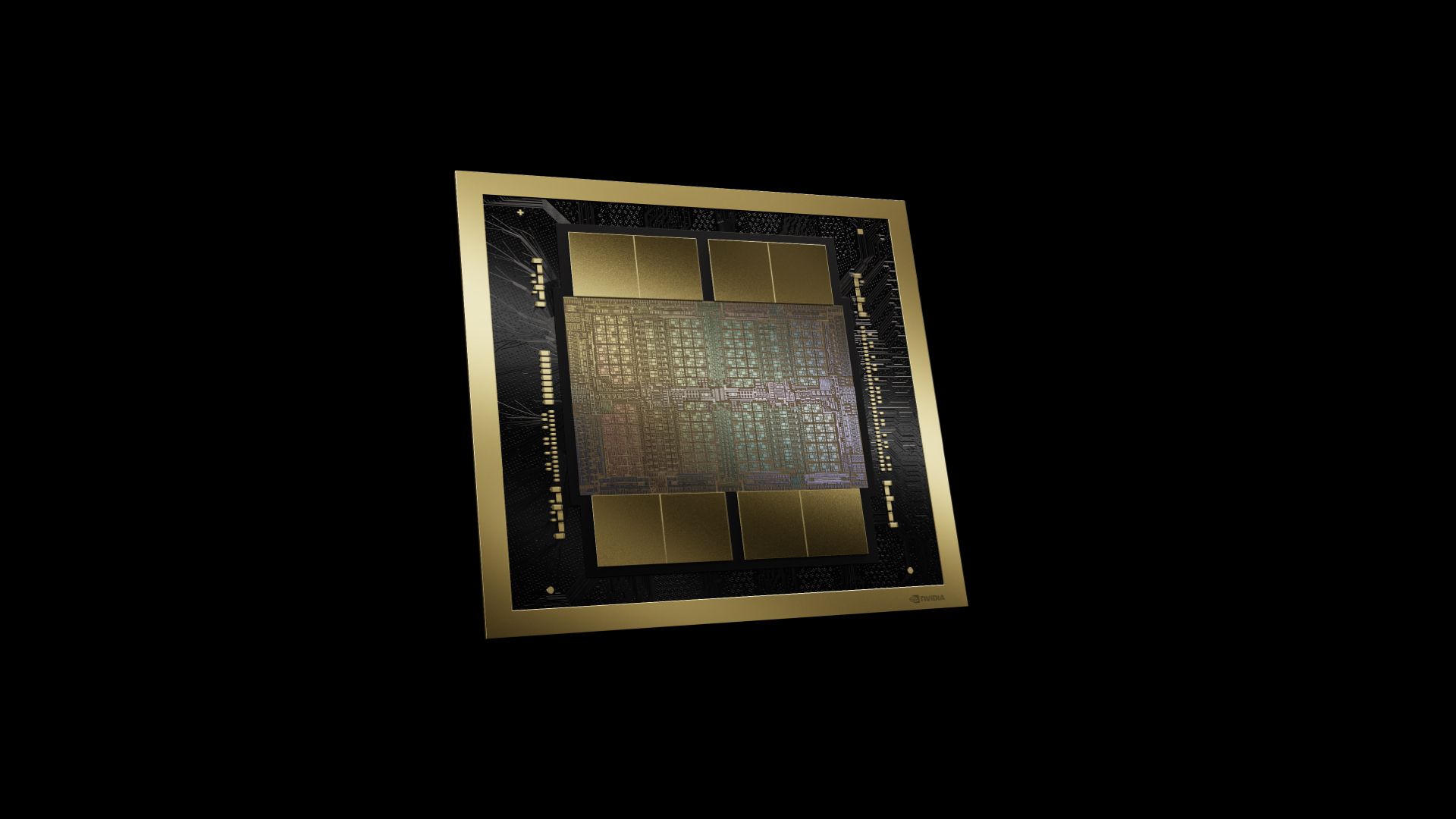
The device itself, revealed at ITF World, uses silicon quantum dot spin qubits. These aren’t your granddad’s transistors; they’re nanoscale traps for individual electrons, manipulating their quantum spin states to hold information. What’s mind-blowing is the precision: gate gaps of a mere 6 nanometers. That level of detail is what separates a promising concept from something that could actually scale.
Why This Isn’t Just About Raw Power
Sure, quantum computers promise to obliterate problems that would take today’s supercomputers eons to even sniff. But for decades, the bottleneck hasn’t been the idea of quantum computing; it’s been the sheer, unadulterated difficulty of building them. We’ve seen countless architectures – superconducting, trapped ions, photonics – and while they all show promise, scaling them into machines with the millions of reliable, controllable qubits needed for true fault tolerance has been the Everest of engineering. Imec’s announcement targets this precisely. They’re saying, “Forget just the physics; let’s talk about making these things in bulk.”
The Manufacturing Metamorphosis
The core genius here lies in imec’s approach: silicon quantum dot spin qubits. These are often dubbed “industry qubits” for a very good reason. The dream is to use the decades of colossal investment and refined expertise the semiconductor industry has poured into CMOS manufacturing. Instead of building entirely new, exotic fabrication ecosystems from scratch, the idea is to hitch a ride on the established manufacturing gravy train. It’s like using an existing, hyper-efficient airport to launch your new experimental rocket, rather than trying to build a whole new spaceport.
At the heart of it, these qubits trap electrons in tiny silicon structures. Their spin state is the bits of quantum information, and surrounding metallic gates nudge and prod them into interacting with their neighbors. Simple in concept, astronomically difficult in execution. The closer these quantum dots are, the stronger their quantum connection – improving control and accuracy. But achieving this proximity demands an almost impossible level of precision in patterning minuscule gaps.
Imec claims to have hit that sweet spot, fabricating arrays with just 6nm gaps between control gates, all thanks to the newest tool in the semiconductor arsenal: High-NA EUV lithography.
High-NA EUV: The Future, Now
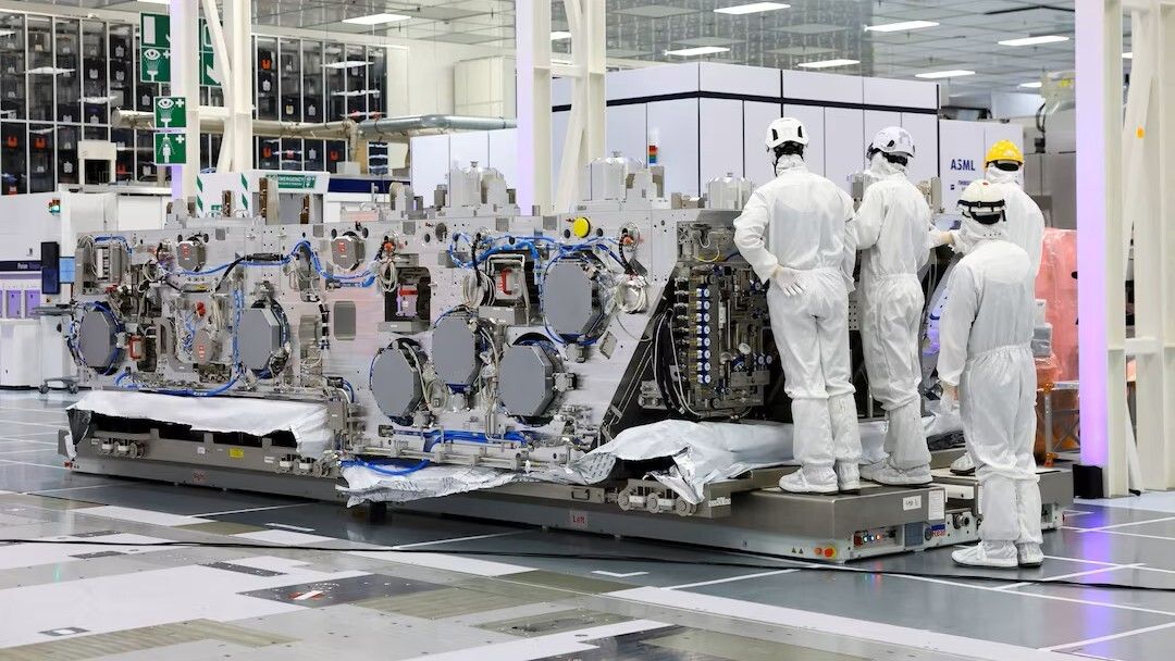
For those not deep in the silicon trenches, High-NA EUV is the next evolution of lithography, the process of printing incredibly fine patterns onto silicon wafers. It’s built by ASML, and it’s designed for the sub-2nm chips that will power our future AI accelerators and dense memory. This new generation cranks up the precision, allowing for dramatically smaller and more faithful features than even current EUV machines can manage. The key jump? A leap in numerical aperture from 0.33 to 0.55. This might sound like a small spec, but in the world of nanometer-scale manufacturing, it’s a chasm.
These machines themselves are monuments to human ingenuity and industrial ambition. Weighing around 150 tons and stretching the length of a double-decker bus, they feature redesigned optical systems with mirrors that are larger, heavier, and polished to an almost unimaginable atomic precision by ZEISS. This isn’t an upgrade; it’s a ground-up reinvention.
Even within the mainstream chip-making world, High-NA EUV is just starting its journey. Intel, for instance, has been an early adopter, integrating the first of these behemoths. But imec’s move to employ it for quantum dots is a stunning signal. It suggests a convergence where the most advanced quantum hardware development isn’t just parallel to AI hardware development, but is actively joining its manufacturing roadmap.
A Bold Prediction: Quantum Computers on Our Desks by 2035?
If this imec breakthrough validates and scales, we’re looking at a potential paradigm shift in quantum computing timelines. For years, the consensus has been that commercially viable, fault-tolerant quantum computers are a 2030s, maybe even 2040s, affair. But what if piggybacking on the AI chip manufacturing roadmap – a roadmap that’s accelerating at a breakneck pace thanks to intense competition and massive investment – can shave years, or even a decade, off that?
My own take? We’re not talking about personal quantum laptops tomorrow, but the idea of specialized, powerful quantum co-processors integrated into data centers or even high-end workstations for specific problem sets becomes far more tangible. Imagine scientific research, drug discovery, or complex financial modeling being augmented by local quantum capabilities within the next 10-15 years. This announcement feels like the ignition switch for that future. It’s the first real evidence that quantum hardware can plug into the existing, lightning-fast innovation cycle of the semiconductor industry, rather than being stuck in its own slow-moving research lane. The implications for AI itself are also staggering – think quantum-enhanced AI algorithms.
“We believe that High-NA EUV lithography has the potential to bring quantum computing manufacturing onto the same roadmap as next-generation AI processors, significantly compressing the timelines for achieving large-scale, fault-tolerant quantum computers.” - Imec Spokesperson (paraphrased from context)
This isn’t just about faster computers; it’s about a foundational shift in how we build them. The semiconductor industry’s relentless pursuit of smaller, faster, and more efficient chips for AI and high-performance computing has just gifted the quantum world a potential shortcut. It’s an exciting, perhaps even bewildering, moment. The future of computation is looking less like separate tracks and more like a single, incredibly fast, technologically converged highway.
🧬 Related Insights
- Read more: Flutter Apple Sign In Error 1000: The Xcode Glitch That Silently Kills Your iOS Auth
- Read more: Budget Android Phones Are Shipping Straight from Factories with Firmware Malware
Frequently Asked Questions
What does High-NA EUV lithography enable for quantum computing? High-NA EUV lithography allows for the fabrication of quantum dot qubits with extremely small and precise features, like the 6nm gate gaps achieved by imec. This increased precision is crucial for scaling up quantum computers by enabling tighter control and better interaction between qubits, mirroring advancements in next-generation AI processors.
How does imec’s quantum dot qubit differ from other quantum computing technologies? Imec’s approach uses silicon quantum dot spin qubits, which aim to use existing CMOS semiconductor manufacturing infrastructure. This is a significant departure from some other quantum computing technologies that rely on more exotic, standalone fabrication processes, potentially making imec’s method more scalable and cost-effective in the long run.
Will this new quantum computing technology make AI processors faster? This development primarily accelerates quantum computing hardware. However, it could indirectly benefit AI by enabling quantum-enhanced AI algorithms and by potentially creating a unified manufacturing roadmap for both advanced quantum and AI processors, leading to shared technological advancements and faster overall progress in computing.