Clay PCBs: A Prehistoric Leap for DIY Hardware
Forget sterile labs and plastic PCBs. A radical new project is digging into the earth, not just for materials, but for a fundamental shift in how we build electronics.
⚡ Key Takeaways
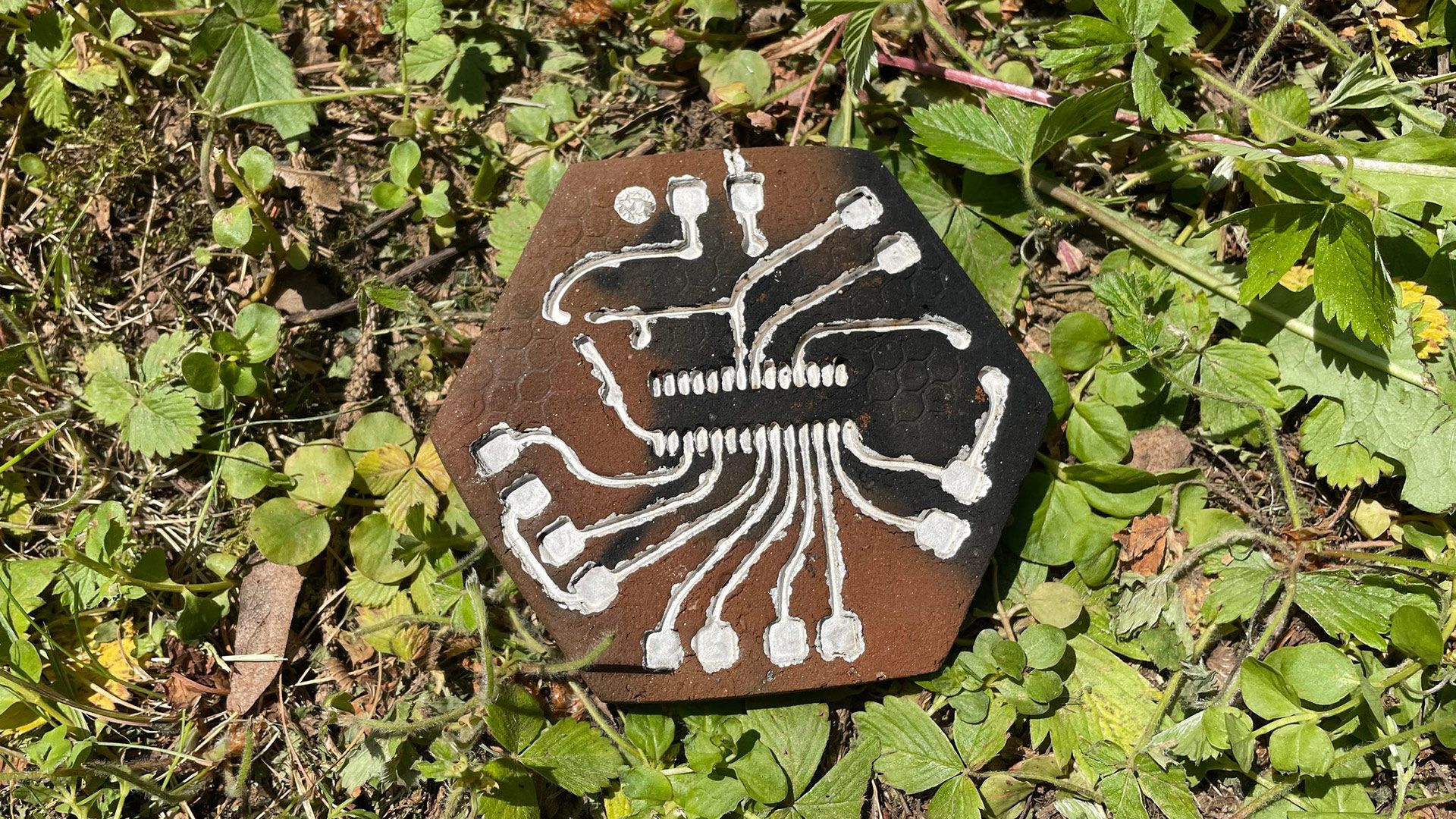
- Hacktivists have developed a method to create functional PCBs using natural clay and ancient firing techniques. 𝕏
- The project prioritizes ethical sourcing, avoiding conflict minerals and utilizing recycled silver for traces. 𝕏
- All project details and resources are open-sourced, encouraging community participation and further development. 𝕏

Worth sharing?
Get the best AI stories of the week in your inbox — no noise, no spam.
Originally reported by Tom's Hardware - AI
Related Stories
AI Hardware
Intel: Up to 30% Game Performance Hiding in Your CPU!

AI Hardware
Anthropic's $500M Silicon Sprint: Nvidia's Fortress Starts to Crumble
AI Hardware
China's Nvidia Partner Grabs $92M in Banned AI Servers — Super Micro Smuggling Shocker Hits Shares

AI Hardware